Ultrafast Laser Synthesis of Nanomaterials and Device Components
Ultrafast laser processing is a promising tool for the fabrication of nanomaterials of different morphologies, as well as device components, for multiple applications ranging from solar cells and automotive sensors to biomedical devices.
Activities:
Ultrafast Laser Synthesis of Nanomaterials and Device Components
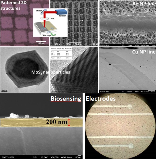
Ultrafast laser processing is a promising tool for the fabrication of nanomaterials of different morphologies, as well as device components, for multiple applications ranging from solar cells to biomedical devices. According these lines, two-dimensional (graphene-based) or other low-dimensional (MoS2 and WS2, fullerene-like and nanotubes) as well as perovskite nanostructures and device components can be fabricated.
Activities:
a) Laser fabrication of graphene-based materials and device components for photovoltaic and biomedical applications
Photochemical techniques have been introduced for the fabrication and modification of graphene-based materials for the enhancement of the photovoltaic devices’ performance. These materials can be used in organic electronics, particular to organic photovoltaics, field effect transistors and electron emission cathodes. In particular, a reduction technique using a femtosecond laser compatible with flexible, temperature sensitive substrates, have been utilized for the production of transparent conductive flexible graphene electrodes [1]. The charge transport properties of such layer can be further improved with a simultaneous reduction and doping with Cl or N through pulsed UV irradiation in liquid or gas media. Furthermore, a laser-based patterning technique has been developed for the production of large area reduced graphene oxide micromesh (rGOMM) electrodes for advanced photovoltaics [2].
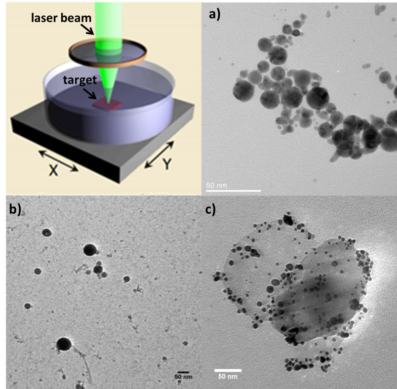
Laser-induced techniques in colloidal medium have been also used to decorate the 2D materials with metallic or semiconducting nanoparticles (NPs) [3]. The second material has been synthesized with laser ablation techniques or colloidal wet chemistry methods. The hybrid systems have been designed in order to exploit both the contribution of NPs in the light absorption enhancement and the band gap tunability of the 2D materials. This could lead to higher exciton dissociation and charge collection in photovoltaic devices. It has been shown that few seconds of UV irradiation is sufficient to decorate the nanosheets lattice with NPs, while the nanoparticles density can be readily controlled upon variation of the irradiation time.
The laser reduced graphene-based electrodes could be also applied in biomolecular sensing and drug delivery applications. Brain function relies upon a complex, coordinated function of neurons, glial cells and blood vessels, which in neurological disorders such as epilepsy, Alzheimer’s, and Parkinson’s disease, is disrupted. Within the EPIGRAPH [4] project we aim the design and develop graphene biomolecular sensors, with graphene organic electronic ion pump neurotransmitter delivery and electrophysiological electrodes, integrated in an “all-in-one or single device/platform” for the prediction and control of epileptic seizures (towards a general intervention tool for most brain disorders).

b) Laser sintering of metallic and dielectric nanoinks for energy, smart food packaging and automotive sensors applications.
In the SINTERINK project we developed the technology in operational environment for a manufacturing process incorporating digital multilayer inkjet conductive and dielectric printing complemented by direct laser sintering. The process can be used for the fabrication of inkjet-printed metallic grids for photovoltaics as well as dielectrics for embedded capacitors.
In products such as fresh meat, chicken, fish and fruit and vegetables during the catabolism process gases are produced mainly of CO2 but also nitrogenous compounds such as trimethylamine, dimethylamine ethylamine and ammonia (NH3). In the SMARTPACK project we develop CO2 and NH3 sensors with appropriate nanoparticle inks using modern, low-cost printing technologies combined with laser sintering to monitor the conditions of the packaged food during its distribution and self-displacement.
Finally, autonomous driving and self-driving cars are important use cases for microelectronics and sensors and most importantly, radio detection and ranging (RADAR) and light detection and ranging (LiDAR) sensors. Such high-value and high-performance systems are necessary for advanced driver-assistance systems as well as for completely autonomous cars. The TINKER project if focused in two main objectives: establishing a pilot platform based on additive manufacturing techniques andand showing the platform’s potential by fabricating the sensor packages themselves. Within the TINKER framework, FORTH has designed the new laser sintering module for industrial purposes and is anticipating optimising it for implementation into the Inkjet printer system. The laser sintering module will ensure local optical energy distribution over the ink patterns avoiding damage of heat sensitive substrates at speeds up to 7000mm/sec [5].
c) Laser synthesis of low-dimensional materials:
Laser-ablation techniques with ultrashort pulses have been employed for the fabrication of fullerene-like MoS2 NPs as well as of WS2 nanotubes. The suggested method is simple and cost efficient as no high cost vacuum facilities are required. These findings open up great opportunities for the synthesis and study of new kinds of inorganic nanostructures with properties that may differ significantly from the corresponding bulk materials. Various potential applications ranging from catalysis and electronics to solar cells and drug delivery have been proposed for these low dimensional materials as they exhibit excellent solid lubrication behaviour.
References:
1. E. Kymakis, K. Savva, M. M. Stylianakis, C. Fotakis, E. Stratakis, Flexible Organic Photovoltaic Cells with In Situ Nonthermal Photoreduction of Spin-Coated Graphene Oxide Electrodes, Adv. Funct. Mater. 2013, 23, 2742.
2. D. Konios, C. Petridis, G. Kakavelakis, M. Sygletou, K. Savva, E. Stratakis, et al. Photovoltaics: Reduced Graphene Oxide Micromesh Electrodes for Large Area, Flexible, Organic Photovoltaic Devices, Adv. Funct. Mater. 2015, 25, 2206.
3. D. Konios, G. Kakavelakis, C. Petridis, E. Stratakis, E. Kymakis, High efficient organic photovoltaic devices utilizing work-function tuned graphene oxide derivatives as the anode and cathode charge extraction layer Journal of Materials Chemistry A, 4, 1612-1623, 2016
4. EPIGRAPH: GRAPHene biomolecular and electrophysiological sensors integrated in an “all-in-one device” for the prediction and control of EPIleptic seizures (towards a general device for most brain disorders), FLAG–ERA JTC 2017, European Reference Code: 26632, National Reference Code: Τ8ΕΡΑ2-00008.
5. M. Chopart, L. Schranzhofer, B. Polzinger, E. Stratakis, M. Pervolaraki and D. Volk, Sensor packages for autonomous cars enabled by additive manufacturing, No 38, OPE journal, March 2022.
